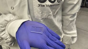
The UNC is home to an array of highly sophisticated electron and scanning probe microscopes, featuring complementary analytical tools for the analysis of nanoscale materials.A newly opened Unit for Nanoscopic Characterization at the Hebrew University in Jerusalem will contribute to Israel’s ability to play a major role in the world scientific arena.
According to the university president Menachem Megidor, “This center is an excellent example of how the understanding of basic science has the potential to promote huge and important applications. Building the UNC has been fascinating and gratifying, and we are happy to do it.”
The UNC provides state-of-the-art technology for analyzing materials and structures at the nanometer (one billionth of a meter) scale, and serves to keep the Hebrew University among the growing number of academic institutions that perform practical research in this area. It is part of the University’s Center for Nanoscience and Nanotechnology.
The UNC opening ceremony was purposefully planned to coincide with the start of a three-day conference entitled, Science and Applications of Nanostructures. Hundreds of researchers and faculty from institutions worldwide arrived at the Givat Ram campus to participate.
The conference included sessions on structures and devices, biotechnology, physics, tools and materials. Along with the Hebrew University and other Israeli academic institutes, lecturers also arrived from Stanford University, the University of California, Georgia Tech, the Swiss Federal Institute of Technology, and the FHI Max Plank Institute.
Uri Banin, a director of the Center, declared the primary mission of the UNC and subsequent planned units to be the development – together with other institutions and Israeli industries – of practical applications and products, as well the education of students from a wide spectrum of University programs. Banin said that at present, there are approximately 20 research groups from diverse disciplines using the Center.
Nanotechnology and nanoscience are increasingly envisioned as drivers for a global industrial revolution that is expected to transform the way many existing products – from clothing to computer chips – are manufactured. Nanotechnology will also create generations of radically efficient and imaginative new products in coming decades.
Attendees were given tours of the $5 million facility, which is housed in modest quarters, occupying 290 square meters of a storage facility for the University’s Purchasing Department. According to Inna Popov, Head of the UNC, the building was selected because it required a minimum of renovation work to assume its new function.
Approximately $3 million of the UNC’s cost was provided by the Yeshaya Horowitz Association, with the remaining amount provided by the University and its commercial technology transfer company, Yissum. Yissum will promote the licensing of patents and intellectual property resulting from research performed at the UNC.
The UNC is home to an array of highly sophisticated electron and scanning probe microscopes, featuring complementary analytical tools for the analysis of nanoscale materials:
** two scanning electron microscopes (SEMs) for examining solids and liquids such as metals, semiconductors, insulators and polymers at resolutions as small as 1.5 nanometers;
** a transmission electron microscope (TEM) for analyzing the composition and structure of defects, interfaces, surfaces, and boundaries of materials at resolutions as small as 2.4 Angstrom points;
** a scanning probe microscope (SPM) for measuring topography and mapping electrical, magnetic and mechanical properties of materials at the nanometer scale;
** an x-ray diffractometer (XRD) for analysis of powders, liquids, and thin layers;
** an x-ray photoelectron spectroscope (XPS) with auger spectroscopy (ESCA) for identifying the basic elements present in materials at special resolutions as low as 100 nanometers.
In addition, the facility provides an on-site lab for preparation of nanoscale samples, as well as access to University computing resources.
In coming years, a nanofabrication unit is also planned for University’s Center for Nanoscience and Nanotechnology. Researchers will use this unit to prepare and test nanoscale devices intended for practical applications, particularly in the manufacture of advanced technology products.
At the opening of the three-day conference, Amir Elstein, Co-General Manager at Intel Israel’s Jerusalem plant, delivered an address on emerging nanotechnologies and nanoscale microelectronics. Elstein noted that in coming months, Intel is poised to begin commercial production of a new generation of transistors that are 50 nanometers in size – about the dimensions of a virus. Though these are the smallest computing devices ever to be manufactured, Elstein said that they represent only the beginning of nanotechnology’s influence in the microelectronics industry.
Uzi Landman, director of Georgia Tech’s Center for Computational Materials Science, also served as a keynote speaker at the opening ceremony. His presentation, entitled “Small is Different”, showed that even dry and technical physics topics can be entertaining. During a lecture in which he bounded repeatedly from one end of the conference stage to another, Landman illustrated novel aspects of atomic behavior that emerge at the nanoscale. Opting for a low-tech delivery on an old-fashioned overhead projector, Landman revealed his award-winning molecular simulation research. At times, he compensated for misplaced slides with lightning-speed puns and vaudevillian showmanship, helping to open the conference and the UNC on an upbeat note.


